XJFlash 
XJFlash is an advanced and innovative method for In-System Programming (ISP) of flash devices through JTAG.
Using XJFlash you can achieve flash programming speeds up to 50 times faster than those possible using conventional boundary scan techniques.

- High-speed flash programming
- Fast firmware upgrade
Custom Solutions – Automatically Generated
XJFlash allows you to automatically generate customised programming solutions for the flash devices connected to FPGAs on your board.
The functional capabilities of the FPGA are harnessed to provide the fastest possible programming speeds. XJFlash automatically generates a custom design for each FPGA/flash combination, allowing you to achieve the best programming times, whilst not requiring you to do any FPGA development.*
Whether you are using SPI, QSPI or parallel NOR flash connected to an FPGA from Altera, Xilinx, Microsemi or Lattice – XJFlash will provide you with a programming solution optimised for your board.
*A licensed version of the relevant FPGA manufacturer’s tools will be required during the configuration of XJFlash. Free versions are sufficient for many devices.
Test Integration
XJFlash is fully compatible with the rest of the XJTAG development system. All XJFlash programming can be run as part of an XJRunner boundary scan test project.
Configurable Flash Programming
It doesn’t matter whether you need to program a single flash device, or multiple devices that are connected in series, to expand the address space, or in parallel, to make a wider data bus, you can use XJFlash to speed up your programming operations.
Custom development
XJFlash can also be used for standalone programming requirements including direct access to I²C and SPI busses or custom protocols such as Microchips ICSP.
The required connections do not need to come from an FPGA on the target board. Providing the protocol signals are available on a header on that board, it should be possible to use XJFlash to achieve fast programming as part of an XJTAG solution.
Please contact us for more details of this service.
Key benefits
- Cuts flash programming times
- SPI, QSPI, parallel NOR flash devices supported
- Support for NAND flash devices available on request
- Shortens development cycles
- No need for additional equipment
- Can be used for fast firmware upgrade
- No FPGA development required
Flexible Licensing Options
- Hardware licence
– held in the JTAG controller so you can use XJTAG on any number of PCs - Network licence
– held on a networked license server available from anywhere in the world
Can I use XJFlash?
In order to use XJFlash all of the data, address and control signals on the flash device(s) must be connected to an FPGA on the target board. This can be a configuration PROM, or a flash device connected to any general purpose I/O pin. These connections can be direct, indirect, dedicated or shared:
Direct connections – YES

The flash is directly connected to the FPGA.
Indirect connections – YES

- The flash is connected to the FPGA via a buffer
- Some of the address signals are shared with the data signals and connected via a latch.
- There is another configurable device, such as a CPLD between the flash and the FPGA.
Shared connections – YES

The flash is connected to the FPGA in one of the modes described above but these connections are shared with another device (such as a processor).
NO connections – YES (with design changes)

If your design contains an FPGA but the flash is not connected in any of the configurations described, it may be possible to use spare pins on the FPGA to establish connections to the flash. These connections would not be used in the mission mode of the board but would allow you to use XJFlash to perform fast flash programming. If your FPGA is a slave device on the same address/data bus as the flash, this may not require many extra signals.
NO FPGA – Not directly

Unfortunately, it is not possible to use XJFlash if there is no FPGA, but it may be possible to do fast flash programming using the debug interface on a processor – please contact us see if you can use this approach on your board.
Alternatively, if it is possible to bring the connections of the flash to a header on the board, XJFlash fast programming can be performed directly via that connector.
XJFlash Example Timings
Minimum theoretical time for conventional boundary scan: 35 minutes.
Total XJFlash run time: 10.5 s to 32.6 s.
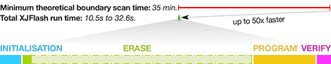
XJFlash will automatically step through four stages each time a flash device is programmed:
Initialisation – The FPGA connected to the flash is configured with the XJFlash image required for the target board. Example time: 2.1 s.
Erase – The flash can be erased using one of two algorithms. The basic erase will simply erase all blocks within a defined range (this may be the whole flash or just the space needed for the image to be programmed). The more intelligent erase will use the fact that it is quicker to read the flash than to erase it; as such it reads from each address and only starts erasing if some data is found. This step can be skipped if it is known that the flash will always be blank before it is programmed.
Example time - intelligent erase enabled: 0.9 s with a device already erased, to 23 s with a fully programmed device (limited by erase time of device).
Program – Data from the target images is streamed into the FPGA through its JTAG port. The FPGA then programs this data into the connected flash(s). Multiple files can be specified and programmed at defined offsets. This step can be bypassed if only verification is required.
Example time: 6.2 s (limited by the programming speed of the device).
Verify – The verification checks every byte in the flash against the specified file(s), ensuring there are no data bit errors. This step can be bypassed if only programming or erasing is required.
Example time: 1.8 s with TCK at 10 MHz, reducing to 1.3 s with TCK at 20 MHz.
These example times are provided for a Spartan 6 XC6SLX9 programming a 2 MByte pseudo-random data file into the FPGA’s SPI configuration PROM.
Compatibility
- Altera – Arria GX, Arria II GX, Arria II GZ, Cyclone, Cyclone II, Cyclone III, Cyclone III LS, Cyclone IV E, Cyclone IV GX, Stratix, Stratix GX, Stratix II, Stratix II GX, Stratix III, Stratix IV
- Lattice – MachXO2, LatticeECP3, LatticeXP2
- Microsemi – ProASIC3, ProASIC3E, ProASIC3L
- Xilinx – Spartan3, Spartan3a, Spartan3e, Spartan6, Virtex4, Virtex5, Virtex6
This list is continuously growing, so contact us for the latest details.
Recommended system requirements
- Intel® Core i3, i5, i7 processor or equivalent (any generation)
- Microsoft® Windows® 7 or Windows 8 (32 or 64 bit)
- 4 GB of RAM
Frequently asked questions
General
- How can XJFlash be 50 times faster than programming with conventional boundary scan?
- I use a fast flash programmer already, why should I consider using XJFlash?
Technical questions
- What flash devices are supported?
- What if I want to program a type of device that's not listed?
- What FPGAs are supported?
- Can I use XJFlash on boards I’ve already designed?
- My flash is not connected directly to the FPGA on my board, might I still be able to use XJFlash?
- Not all the signals on my flash are accessible from the FPGA, surely that makes it impossible to use XJFlash?
- Is this limited to only programming FPGA configuration devices?
- I’m not an FPGA developer, will this be too complicated for me?
- Will I have to buy extra FPGA tools to be able to use XJFlash?
- Can I simultaneously program multiple PCBs, each with their own flash devices?
- Can I use XJFlash both in high-volume and low-volume/high-mix production situations?
- This can’t be faster than the FPGA vendor’s programming tool, can it?
- Do you support fast Flash programming attached to microprocessors, CPUs, DSPs?
- What are the recommended system requirements to run XJFlash?