Cadence OrCAD FPGA System Planner
Innovative FPGA-PCB Co-Design
The Cadence® OrCAD® FPGA System Planner provides a complete, scalable solution for FPGA-PCB co-design that allows users to create an optimum correct-by-construction pin assignment. FPGA pin assignment is synthesized automatically based on user-specified, interface-based connectivity (design intent), as well as FPGA pin assignment rules (FPGA-rules), and actual placement of FPGAs on PCB (relative placement). Read more on the FPGA System Planner launch announcement.
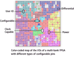
 Integrating today’s large-pin-count FPGAs – with their many different types of user-configurable pins and assignment rules – extends the time to create optimal pin assignment. Often the assignment is done manually at a pin-by-pin level in an environment that is unaware of the placement of critical PCB components that are connected to FPGAs. Without understanding the impact to PCB routing, FPGA-based design projects are forced to choose between two poor options: live with suboptimal pin assignment, which can increase the number of layers on a PCB design; or deal with several unnecessary iterations at the tail end of the design cycle. Even with several iterations, this manual and error-prone approach can result in unnecessary PCB design re-spins.
The OrCAD FPGA System Planner is integrated with both OrCAD Capture and OrCAD PCB Editor. It reads and creates OrCAD Capture schematics and symbols. In addition, a floorplan view uses existing footprint libraries from OrCAD PCB Editor. Should placement change during layout, pin optimization using FPGA System Planner can be accessed directly from OrCAD PCB Editor.
Features/Benefits
- Scalable, cost-effective FPGA-PCB co-design solution from OrCAD to Cadence Allegro® GXL
- Shortens time for optimum initial pin assignment, accelerating PCB design schedules
- Accelerates integration of FPGAs with OrCAD PCB design creation environments
- Eliminates unnecessary, frustrating design iterations during the PCB layout process
- Eliminates unnecessary physical prototype iterations due to FPGA pin assignment errors
- Reduces PCB layer count through placement aware pin assignment and optimization
Scalability
The OrCAD and Allegro FPGA System Planner technology is available in the following product offerings:
- Allegro FPGA System Planner GXL – for synthesizing and optimizing pin assignment of more than four FPGAs at a time
- Allegro FPGA System Planner XL – for concurrent pin assignment, synthesis and post-placement optimization of up to four FPGAs at a time
- Allegro FPGA System Planner L – for pin assignment synthesis and post-placement optimization of a single FPGA
- OrCAD FPGA System Planner – for optimum initial pin assignment synthesis of a single FPGA
Additional Info & Sales
The OrCAD product line is owned by Cadence Design Systems. Sales, support, services, and training for the OrCAD product line are provided through a global network of Cadence Channel Partners (VARs).
